1
Data sheet acquired from Harris Semiconductor
SCHS148A
Features
∑ Multifunction Capability
- Binary to 1 of 4 Decoders or 1 to 4 Line
Demultiplexer
∑ Active Low Mutually Exclusive Outputs
∑ Fanout (Over Temperature Range)
- Standard Outputs . . . . . . . . . . . . . . . 10 LSTTL Loads
- Bus Driver Outputs . . . . . . . . . . . . . 15 LSTTL Loads
∑ Wide Operating Temperature Range . . . -55
o
C to 125
o
C
∑ Balanced Propagation Delay and Transition Times
∑ Significant Power Reduction Compared to LSTTL
Logic ICs
∑ HC Types
- 2V to 6V Operation
- High Noise Immunity: N
IL
= 30%, N
IH
= 30%of V
CC
at
V
CC
= 5V
∑ HCT Types
- 4.5V to 5.5V Operation
- Direct LSTTL Input Logic Compatibility,
V
IL
= 0.8V (Max), V
IH
= 2V (Min)
- CMOS Input Compatibility, I
l
1
µ
A at V
OL
, V
OH
∑ Memory Decoding, Data Routing, Code Conversion
Description
The CD74HC139 and CD74HCT139 devices contain two
independent binary to one of four decoders each with a
single active low enable input (1E or 2E). Data on the select
inputs (1A0 and 1A1 or 2A0 and 2A1) cause one of the four
normally high outputs to go low.
If the enable input is high all four outputs remain high. For
demultiplexer operation the enable input is the data input.
The enable input also functions as a chip select when these
devices are cascaded. This device is functionally the same
as the CD4556B and is pin compatible with it.
The outputs of these devices can drive 10 low power
Schottky TTL equivalent loads. The 74HCT logic family is
functionally as well as pin equivalent to the 74LS logic family.
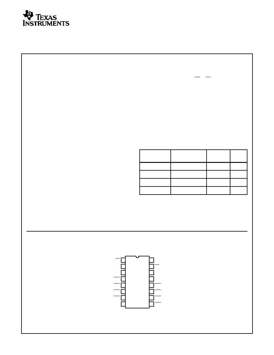
Pinout
CD74HC139, CD74HCT139
(PDIP, SOIC)
TOP VIEW
Ordering Information
PART NUMBER
TEMP. RANGE (
o
C)
PACKAGE
PKG.
NO.
CD74HC139E
-55 to 125
16 Ld PDIP
E16.3
CD74HCT139E
-55 to 125
16 Ld PDIP
E16.3
CD74HC139M
-55 to 125
16 Ld SOIC
M16.15
CD74HCT139M
-55 to 125
16 Ld SOIC
M16.15
NOTES:
1. When ordering, use the entire part number. Add the suffix 96 to
obtain the variant in the tape and reel.
2. Die is available which meets all electrical specifications. Please
contact your local sales office or customer service for ordering
information.
14
15
16
9
13
12
11
10
1
2
3
4
5
7
6
8
1E
1A0
1A1
1Y0
1Y1
1Y2
GND
1Y3
V
CC
2A0
2A1
2Y0
2Y1
2Y2
2Y3
2E
September 1997 - Revised May 1999
CAUTION: These devices are sensitive to electrostatic discharge. Users should follow proper IC Handling Procedures.
Copyright
©
Texas Instruments Incorporated 1999
CD74HC139,
CD74HCT139
High-Speed CMOS Logic
Dual 2-to-4 Line Decoder/Demultiplexer
[ /Title
(CD74
HC139
,
CD74
HCT13
9)
/Sub-
ject
(High
Speed
CMOS
Logic
Dual
2-to-4
Line
Decod
2
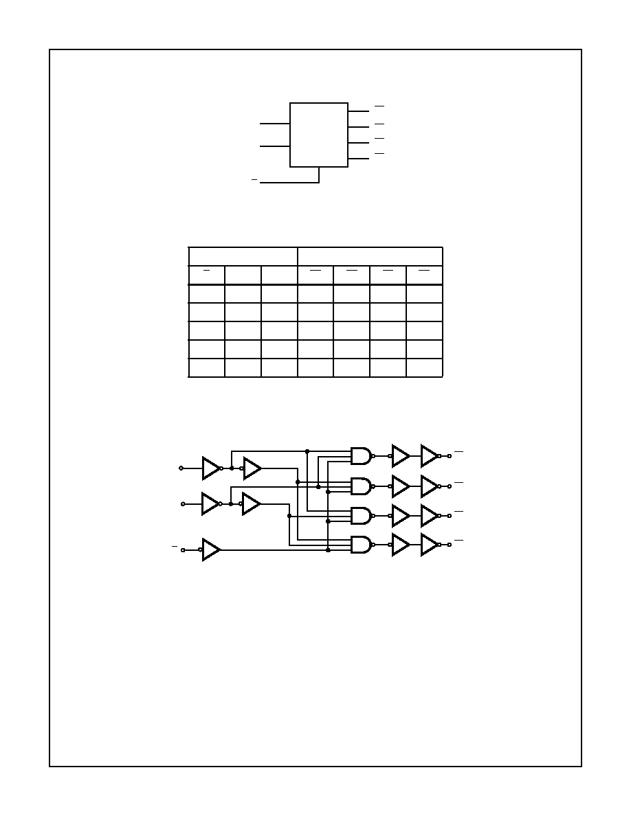
Functional Diagram
Logic Diagram
TRUTH TABLE
INPUTS ENABLE SELECT
OUTPUTS
E
A1
A0
Y3
Y2
Y1
Y0
0
0
0
1
1
1
0
0
0
1
1
1
0
1
0
1
0
1
0
1
1
0
1
1
0
1
1
1
1
X
X
1
1
1
1
NOTE: X = Don't Care, Logic 1 = High, Logic 0 = Low
A0
2 (14)
3 (13)
4 (12)
Y3
Y0
A1
1 (15)
E
5 (11)
6 (10)
7 (9)
Y1
Y2
4 (12)
5 (11)
Y0
Y1
6 (10)
Y2
7 (9)
Y3
2 (14)
A0
3 (13)
A1
1 (15)
E
CD74HC139, CD74HCT139
3
Absolute Maximum Ratings
Thermal Information
DC Supply Voltage, V
CC
. . . . . . . . . . . . . . . . . . . . . . . . -0.5V to 7V
DC Input Diode Current, I
IK
For V
I
< -0.5V or V
I
> V
CC
+ 0.5V
. . . . . . . . . . . . . . . . . . . . . .±
20mA
DC Output Diode Current, I
OK
For V
O
< -0.5V or V
O
> V
CC
+ 0.5V
. . . . . . . . . . . . . . . . . . . .±
20mA
DC Output Source or Sink Current per Output Pin, I
O
For V
O
> -0.5V or V
O
< V
CC
+ 0.5V
. . . . . . . . . . . . . . . . . . . .±
25mA
DC V
CC
or Ground Current, I
CC or
I
GND
. . . . . . . . . . . . . . . . . .±
50mA
Operating Conditions
Temperature Range (T
A
) . . . . . . . . . . . . . . . . . . . . . -55
o
C to 125
o
C
Supply Voltage Range, V
CC
HC Types . . . . . . . . . . . . . . . . . . . . . . . . . . . . . . . . . . . . .2V to 6V
HCT Types . . . . . . . . . . . . . . . . . . . . . . . . . . . . . . . . .4.5V to 5.5V
DC Input or Output Voltage, V
I
, V
O
. . . . . . . . . . . . . . . . . 0V to V
CC
Input Rise and Fall Time
2V . . . . . . . . . . . . . . . . . . . . . . . . . . . . . . . . . . . . . . 1000ns (Max)
4.5V. . . . . . . . . . . . . . . . . . . . . . . . . . . . . . . . . . . . . . 500ns (Max)
6V . . . . . . . . . . . . . . . . . . . . . . . . . . . . . . . . . . . . . . . 400ns (Max)
Thermal Resistance (Typical, Note 3)
JA
(
o
C/W)
PDIP Package . . . . . . . . . . . . . . . . . . . . . . . . . . . . .
90
SOIC Package . . . . . . . . . . . . . . . . . . . . . . . . . . . . .
115
Maximum Junction Temperature . . . . . . . . . . . . . . . . . . . . . . . 150
o
C
Maximum Storage Temperature Range . . . . . . . . . .-65
o
C to 150
o
C
Maximum Lead Temperature (Soldering 10s) . . . . . . . . . . . . . 300
o
C
(SOIC - Lead Tips Only)
CAUTION: Stresses above those listed in "Absolute Maximum Ratings" may cause permanent damage to the device. This is a stress only rating and operation
of the device at these or any other conditions above those indicated in the operational sections of this specification is not implied.
NOTE:
3.
JA
is measured with the component mounted on an evaluation PC board in free air.
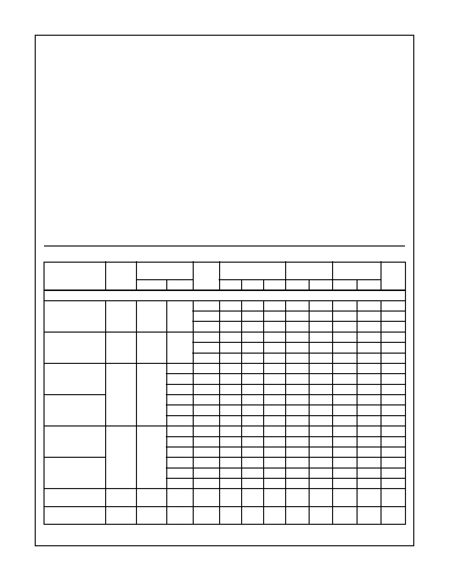
DC Electrical Specifications
PARAMETER
SYMBOL
TEST
CONDITIONS
V
CC
(V)
25
o
C
-40
o
C TO 85
o
C -55
o
C TO 125
o
C
UNITS
V
I
(V)
I
O
(mA)
MIN
TYP
MAX
MIN
MAX
MIN
MAX
HC TYPES
High Level Input
Voltage
V
IH
-
-
2
1.5
-
-
1.5
-
1.5
-
V
4.5
3.15
-
-
3.15
-
3.15
-
V
6
4.2
-
-
4.2
-
4.2
-
V
Low Level Input
Voltage
V
IL
-
-
2
-
-
0.5
-
0.5
-
0.5
V
4.5
-
-
1.35
-
1.35
-
1.35
V
6
-
-
1.8
-
1.8
-
1.8
V
High Level Output
Voltage
CMOS Loads
V
OH
V
IH
or V
IL
-0.02
2
1.9
-
-
1.9
-
1.9
-
V
-0.02
4.5
4.4
-
-
4.4
-
4.4
-
V
-0.02
6
5.9
-
-
5.9
-
5.9
-
V
High Level Output
Voltage
TTL Loads
-
-
-
-
-
-
-
-
-
V
-4
4.5
3.98
-
-
3.84
-
3.7
-
V
-5.2
6
5.48
-
-
5.34
-
5.2
-
V
Low Level Output
Voltage
CMOS Loads
V
OL
V
IH
or V
IL
0.02
2
-
-
0.1
-
0.1
-
0.1
V
0.02
4.5
-
-
0.1
-
0.1
-
0.1
V
0.02
6
-
-
0.1
-
0.1
-
0.1
V
Low Level Output
Voltage
TTL Loads
-
-
-
-
-
-
-
-
-
V
4
4.5
-
-
0.26
-
0.33
-
0.4
V
5.2
6
-
-
0.26
-
0.33
-
0.4
V
Input Leakage
Current
I
I
V
CC
or
GND
-
6
-
-
±
0.1
-
±
1
-
±
1
µ
A
Quiescent Device
Current
I
CC
V
CC
or
GND
0
6
-
-
8
-
80
-
160
µ
A
CD74HC139, CD74HCT139
4
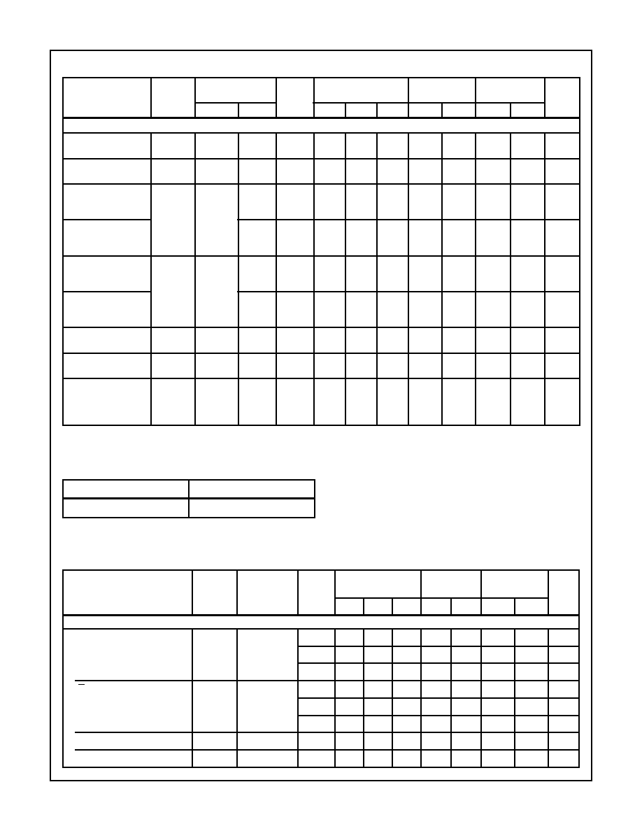
HCT TYPES
High Level Input
Voltage
V
IH
-
-
4.5 to
5.5
2
-
-
2
-
2
-
V
Low Level Input
Voltage
V
IL
-
-
4.5 to
5.5
-
-
0.8
-
0.8
-
0.8
V
High Level Output
Voltage
CMOS Loads
V
OH
V
IH
or V
IL
-0.02
4.5
4.4
-
-
4.4
-
4.4
-
V
High Level Output
Voltage
TTL Loads
-4
4.5
3.98
-
-
3.84
-
3.7
-
V
Low Level Output
Voltage
CMOS Loads
V
OL
V
IH
or V
IL
0.02
4.5
-
-
0.1
-
0.1
-
0.1
V
Low Level Output
Voltage
TTL Loads
4
4.5
-
-
0.26
-
0.33
-
0.4
V
Input Leakage
Current
I
I
V
CC
and
GND
0
5.5
-
±
0.1
-
±
1
-
±
1
µ
A
Quiescent Device
Current
I
CC
V
CC
or
GND
0
5.5
-
-
8
-
80
-
160
µ
A
Additional Quiescent
Device Current Per
Input Pin: 1 Unit Load
(Note 4)
I
CC
V
CC
-2.1
-
4.5 to
5.5
-
100
360
-
450
-
490
µ
A
NOTE:
4. For dual-supply systems theoretical worst case (V
I
= 2.4V, V
CC
= 5.5V) specification is 1.8mA.
DC Electrical Specifications
(Continued)
PARAMETER
SYMBOL
TEST
CONDITIONS
V
CC
(V)
25
o
C
-40
o
C TO 85
o
C -55
o
C TO 125
o
C
UNITS
V
I
(V)
I
O
(mA)
MIN
TYP
MAX
MIN
MAX
MIN
MAX
HCT Input Loading Table
INPUT
UNIT LOADS
All
0.7
NOTE: Unit Load is
I
CC
limit specified in DC Electrical Table, e.g.,
360
µ
A max at 25
o
C.
Switching Specifications
Input t
r
, t
f
= 6ns
PARAMETER
SYMBOL
TEST
CONDITIONS
V
CC
(V)
25
o
C
-40
o
C TO
85
o
C
-55
o
C TO
125
o
C
UNITS
MIN
TYP
MAX
MIN
MAX
MIN
MAX
HC TYPES
Propagation Delay
t
PLH,
t
PHL
C
L
= 50pF
2
-
-
145
-
180
-
220
ns
A0, A1 to Outputs
4.5
-
-
29
-
36
-
44
ns
6
-
-
25
-
31
-
38
ns
E to Outputs
t
PLH,
t
PHL
C
L
= 50pF
2
-
-
135
-
170
-
205
ns
4.5
-
-
27
-
34
-
41
ns
6
-
-
23
-
29
-
35
ns
Select to Output
t
PLH,
t
PHL
C
L
= 15pF
5
-
12
-
-
-
-
-
ns
Enable to Output
t
PLH,
t
PHL
C
L
= 15pF
5
-
11
-
-
-
-
-
ns
CD74HC139, CD74HCT139
5
Output Transition Time (Figure 1) t
TLH
, t
THL
C
L
= 50pF
2
-
-
75
-
95
-
110
ns
4.5
-
-
15
-
19
-
22
ns
6
-
-
13
-
16
-
19
ns
Power Dissipation
Capacitance, (Notes 5, 6)
C
PD
-
5
-
55
-
-
-
-
-
pF
Input Capacitance
C
IN
-
-
-
-
10
-
10
-
10
pF
HCT TYPES
Propagation Delay
A0, A1 to Outputs
t
PLH
,
t
PHL
C
L
= 50pF
4.5
-
-
34
-
43
-
51
ns
E to Outputs
t
PLH
,
t
PHL
C
L
= 50pF
4.5
-
-
34
-
43
-
51
ns
Select to Output
t
PLH,
t
PHL
C
L
= 15pF
5
-
14
-
-
-
-
-
ns
Enable to Output
t
PLH,
t
PHL
C
L
= 15pF
5
-
14
-
-
-
-
-
ns
Output Transition Time
(Figure 2)
t
TLH
, t
THL
C
L
= 50pF
4.5
-
-
15
-
19
-
22
ns
Power Dissipation
Capacitance, (Notes 5, 6)
C
PD
-
5
-
59
-
-
-
-
-
pF
Input Capacitance
C
IN
-
-
-
-
10
-
10
-
10
pF
NOTES:
5. C
PD
is used to determine the dynamic power consumption, per decoder/demux.
6. P
D
= V
CC
2
f
i
(C
PD
+ C
L
) where: f
i
= Input Frequency, C
L
= Output Load Capacitance, V
CC
= Supply Voltage.
Switching Specifications
Input t
r
, t
f
= 6ns (Continued)
PARAMETER
SYMBOL
TEST
CONDITIONS
V
CC
(V)
25
o
C
-40
o
C TO
85
o
C
-55
o
C TO
125
o
C
UNITS
MIN
TYP
MAX
MIN
MAX
MIN
MAX
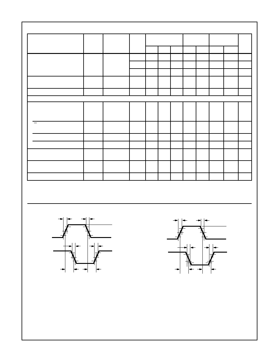
Test Circuits and Waveforms
FIGURE 1. HC AND HCU TRANSITION TIMES AND PROPAGA-
TION DELAY TIMES, COMBINATION LOGIC
FIGURE 2. HCT TRANSITION TIMES AND PROPAGATION
DELAY TIMES, COMBINATION LOGIC
t
PHL
t
PLH
t
THL
t
TLH
90%
50%
10%
50%
10%
INVERTING
OUTPUT
INPUT
GND
V
CC
t
r
= 6ns
t
f
= 6ns
90%
t
PHL
t
PLH
t
THL
t
TLH
2.7V
1.3V
0.3V
1.3V
10%
INVERTING
OUTPUT
INPUT
GND
3V
t
r
= 6ns
t
f
= 6ns
90%
CD74HC139, CD74HCT139

IMPORTANT NOTICE
Texas Instruments and its subsidiaries (TI) reserve the right to make changes to their products or to discontinue
any product or service without notice, and advise customers to obtain the latest version of relevant information
to verify, before placing orders, that information being relied on is current and complete. All products are sold
subject to the terms and conditions of sale supplied at the time of order acknowledgement, including those
pertaining to warranty, patent infringement, and limitation of liability.
TI warrants performance of its semiconductor products to the specifications applicable at the time of sale in
accordance with TI's standard warranty. Testing and other quality control techniques are utilized to the extent
TI deems necessary to support this warranty. Specific testing of all parameters of each device is not necessarily
performed, except those mandated by government requirements.
CERTAIN APPLICATIONS USING SEMICONDUCTOR PRODUCTS MAY INVOLVE POTENTIAL RISKS OF
DEATH, PERSONAL INJURY, OR SEVERE PROPERTY OR ENVIRONMENTAL DAMAGE ("CRITICAL
APPLICATIONS"). TI SEMICONDUCTOR PRODUCTS ARE NOT DESIGNED, AUTHORIZED, OR
WARRANTED TO BE SUITABLE FOR USE IN LIFE-SUPPORT DEVICES OR SYSTEMS OR OTHER
CRITICAL APPLICATIONS. INCLUSION OF TI PRODUCTS IN SUCH APPLICATIONS IS UNDERSTOOD TO
BE FULLY AT THE CUSTOMER'S RISK.
In order to minimize risks associated with the customer's applications, adequate design and operating
safeguards must be provided by the customer to minimize inherent or procedural hazards.
TI assumes no liability for applications assistance or customer product design. TI does not warrant or represent
that any license, either express or implied, is granted under any patent right, copyright, mask work right, or other
intellectual property right of TI covering or relating to any combination, machine, or process in which such
semiconductor products or services might be or are used. TI's publication of information regarding any third
party's products or services does not constitute TI's approval, warranty or endorsement thereof.
Copyright
©
1999, Texas Instruments Incorporated